Japan’s New Semiconductor Offensive
Integrating Semiconductor Research and Production: An Interview with Rapidus President Koike Atsuyoshi (Part 2)
Economy Politics- English
- 日本語
- 简体字
- 繁體字
- Français
- Español
- العربية
- Русский
(Continued from part 1.)
TAKENAKA HARUKATA Rapidus is planning to produce cutting-edge 2-nanometer node logic chips using next-generation gate-all-around technology. How will these advanced semiconductors be used in actual products?
KOIKE ATSUYOSHI First of all, in high-end, high-performance computers. That includes quantum computers. Also, edge computers, which are expected to replace today’s PCs and smartphones. A necessary condition for these computers and other devices is extremely low power consumption. In the age of artificial intelligence, the data-processing capacity of our devices will grow exponentially, but unless we can reduce power consumption, they’ll require big, heavy batteries. That’s why GAA technology is going to be essential.
The Chiplet Challenge
TAKENAKA There’s also been talk about the key role of chiplets—tiny integrated circuits with specific functionalities that are combined to make a single chip. Can you explain the concept to us?
KOIKE The idea of chiplets isn’t anything new; it actually goes back about thirty years. A typical semiconductor chip incorporates all kinds of functions—logic, analog, memory, all embedded in one chip. Until now, semiconductor development has been all about scaling that design to improve performance.
But there has long been some debate as to whether this is the most efficient approach. The first to question this were supercomputer engineers at companies like Fujitsu and IBM. They wondered if it might not make more sense to break chips down into functional modules and then connect and assemble those modules into a package. That was the origin of the chiplet concept.
When you try to embed so many different functions into a single chip, it makes the design extremely complex. And because the performance required from different functions varies, the chip’s overall performance suffers. But if you break it down into modules by function, you can achieve higher performance with smaller chip size, and yield improves. There are lots of pluses. On the other hand, it becomes quite complicated to wire the chiplets together during the back-end process. Furthermore, the development of standards for chiplet technology has proceeded slowly. That’s because chip designers are not accustomed to thinking in terms of manufacturing efficiency.
At Rapidus, we’re aiming to integrate the front-end and back-end processes of semiconductor production. We want to leverage the expertise of manufacturing-savvy engineers to develop a mode of design that optimizes production.

Rapidus President Koike Atsuyoshi (© Hanai Tomoko)
Toward a New Industrial Cluster
TAKENAKA You’ve chosen Chitose in Hokkaidō, Japan’s northernmost island, as the site for your operations. Could you explain the rationale for that choice?
KOIKE There are several basic conditions for the manufacture of semiconductors, including plenty of water, a reliable power supply, and labor. Needless to say, we took all of those factors into account. But the most important requirement for achieving our vision is that we assemble top-caliber, world-class talent. And for that, we felt the key prerequisite was to show Rapidus as a company where people will be eager to come and work.
The city of Chitose offers a fabulous environment. The prefectural government and local business groups recognize that Rapidus is involved in a massive undertaking, and they support it fully.
TAKENAKA In 2021, when TSMC decided to set up production in Japan, it selected Kumamoto, on the southern island of Kyūshū, as its base of operations. Semiconductor-related industries are already clustered in the region, to the point where people refer to Kyūshū as Japan’s Silicon Island. The environment in Hokkaidō is entirely different. What are your thoughts on that score?
KOIKE Of course, Kyūshū is a wonderful place, but for us, there was no advantage in setting up shop there. The competition for human resources would have been too intense. In Hokkaidō right now, you have graduates from Hokkaidō University and other local schools leaving the prefecture because they can’t find work. Rapidus will provide jobs for those people, and we also plan on recruiting talented engineers and researchers from around the world. That will give a big boost to the local economy. Our idea is to attract other chip-related businesses to the region and eventually turn the area encompassing the cities of Tomakomai, Chitose, Sapporo, and Ishikari into Hokkaidō’s own Silicon Valley.
Integrating Semiconductor Research
KOIKE Albany Nanotech Complex, where the semiconductor R&D consortium I mentioned before is based, is part of a state-financed initiative called New York Creates. New York State acquired the land, financed the construction of a university campus, and encouraged corporate partners like IBM to establish research centers there. We’re calling on the Hokkaidō prefectural government to launch a comparable program—“Hokkaidō Creates,” if you like.
When Rapidus was launched, I drew up a corporate philosophy based on “three pillars.” One is human-resource development. The second is development and manufacture with the final product in mind. What I mean by that is that the venture is meaningless unless we can give the world innovative new products by working closely with users while applying the latest semiconductor and chip-design technology. The third pillar is total commitment to greening—minimizing the footprint of manufacturing facilities as well as devices.
I’ve met with the leaders of practically all of Japan’s major universities and explained our philosophy. I’ve also told them that I think we need to integrate the specialized work going on at different institutions—plasma research at Nagoya University, semiconductor design at the University of Tokyo, and so forth. There’s some excellent semiconductor research going on in various departments around the country, but not one of our universities approaches the field holistically. We need something akin to a virtual University of Integrated Semiconductor Studies. And it shouldn’t be limited to Japan. We need to involve US institutions as well. I’ve been talking with people about the possibility of a joint degree program involving top American schools like Rensselaer Polytechnic Institute, Massachusetts Institute of Technology, Stanford, and so forth.
Overwhelmed with Applicants
TAKENAKA You’ve estimated that Rapidus will raise about 2 trillion yen by 2025 and invest another 3 trillion by 2027. Are government subsidies going to constitute the bulk of this funding?
KOIKE There’s no legal guarantee that we’ll actually receive all the money that the government has said it will provide, and in any case, we’re not kidding ourselves that such subsidies will cover the whole cost of the venture. Even if the government supports the R&D phase, we assume we’ll need to raise funds from private companies to start up volume production.
TAKENAKA How are things going in terms of hiring semiconductor engineers? Elsewhere you’ve said that you’ve recruited a lot of Japanese engineers who were working overseas, and that the average age of your employees thus far is about fifty.
KOIKE We’ve been holding monthly induction ceremonies, with about thirty new employees participating each time. It’s true their average age is around fifty, but they’re brimming with youthful zeal. What Rapidus needs now is battle-ready troops, people who know English and can go straight to Albany and master IBM’s technology. We have to complete the technology transfer in two years.
We’ve received so many applications from engineers that we can hardly review them all. But generally speaking, I’ve been impressed by the large number of dedicated engineers who have been working overseas but would dearly love to contribute to the development and production of cutting-edge semiconductors in Japan.
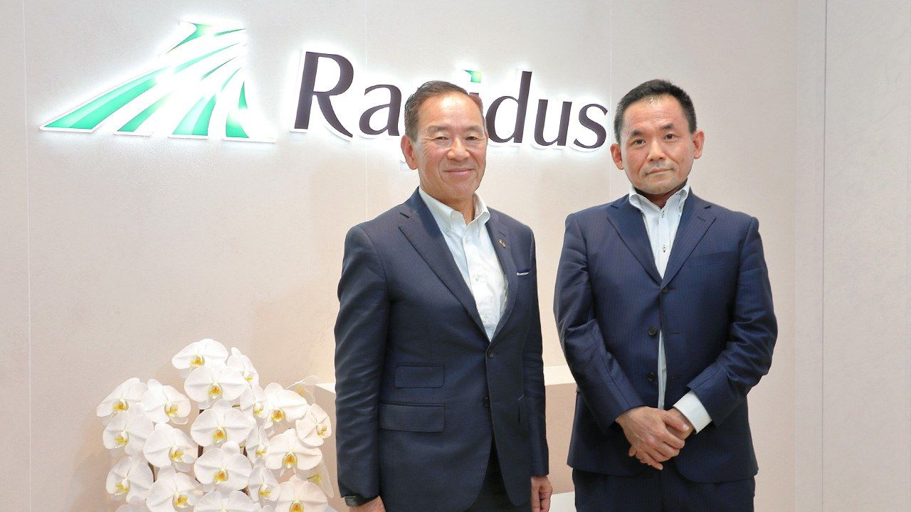
(Originally written in Japanese by Ishii Masato of the Nippon.com Editorial Department based on a July 25, 2023, interview. Banner photo: Rapidus Corp. President Koike Atsuyoshi, left, with Takenaka Harukata, chair of the Nippon.com Editorial Planning Committee, in Tokyo, on July 25, 2023. © Hanai Tomoko.)